ijustpostwhenimhi
1471
12
1

Power is waiting on some smd passives and adapters after a small tweak to the feedback section. I was using through hole passives hoping for convenience, but smds are much cheaper and with a large enough package (1206), it's easy to hand solder them on and off for experimenting.
While I wait, I moved onto placement of the first switch IC. This is a Diodes Incorporated 6 lane/6-port gen3 switch with built-in clock buffer.
The other chip I'll be testing is a Broadcom 12 lane/6-port. I want to start with the DI chip because I can share a lot more info on the process. Broadcom required an NDA, Diodes Inc. did not.

Signal and clock considerations:
All signal and clock pads have no wire wrap pins. The wires will be Molex 85ohm shielded twinax cables, directly soldered to the pads. I have a micro ohmmeter, and plan to attempt to compensate for the adapter traces impedance mismatch. I'll also be adding a bit of grounded shielding tape along the traces. This, plus the chip's built in signal conditioning should be enough to confirm functionality with the pi and downstream devices, albeit maybe not at gen3 speeds for now, but this proto process is to confirm compatibility and familiarize myself with such a circuit in a hands on manner before moving to a PCB design

This is a top view I put together from the datasheet.
Signal and clock pads are green, ground is grey

Underside showing ground committed pins

Datasheet provided bottom view

Cat tax
CrapsMcgee
This is neat. The last time I tried to shorten twinax wires on an msata to u.2 board it never worked.
What do you call that silver proto board?
ijustpostwhenimhi
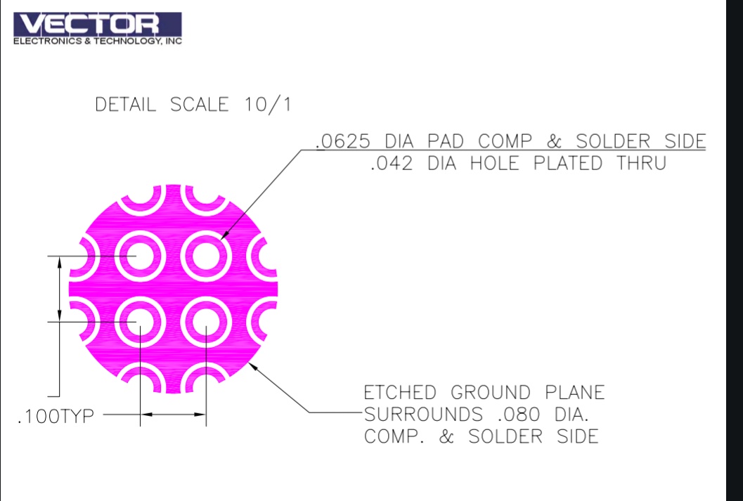
I've had good experience with shortening twinax in DAC cables![]() abit easier than u.2 though. Vector Circboard https://www.vectorelect.com/106p70-4.html
abit easier than u.2 though. Vector Circboard https://www.vectorelect.com/106p70-4.html